Tel: 520.465.1419
E-mail : araca@aracainc.com
We are the exclusive distributor of the patented CARE-TEC® system in North America and Europe. CARE-TEC® is manufactured by Toho Koki Seisakusho Co., Ltd. (Toho) whose chairman, Mr. Tatsutoshi Suzuki, is a co-founder of, and a major strategic investor in, Araca. Through this agreement, Araca will also have access to the CARE-TEC® system at Toho, as well as their state-of-the-art metrology equipment used for determining the crystalline structure, metal contamination, number of surface and sub-surface defects, and the nano-roughness of wide-band-gap (WBG) substrates; all in a brand-new Class 10 cleanroom in Yokkaichi (JP).
For links to the above metrology, please click here and scroll down all the way.
What is CARE-TEC®?
CARE-TEC®, stands for “CAtalyst-Referred Etching Technology”. It is a state-of-the-art load-lock system with four electrochemically assisted polishers, a robotic wafer handling arm, and an integrated substrate cleaning module. The system is uniquely designed to reduce surface smoothness to below 1 nm, while significantly reducing the number of surface and sub-surface defects. Such stringent specifications are crucial for producing epi-ready SiC (and also GaN) substrates. The technology was originally invented by Prof. Yamauchi of Osaka University and has been patented worldwide.

Source: Yamauchi et al., EP 3142142A1 (2017)
CARE-TEC® employs a polymeric pad onto which a catalytic platinum or ruthenium film is sputtered. With just water as the slurry substitute, an electric potential is then applied to the SiC substrate and the pad. The principal mechanism of polishing SiC can be described by the reaction below where SiC is continuously etched away by catalytically converting the top layers of the SiC to monolayers of silicon dioxide which are then removed mechanically (via polishing) at moderate pressures:
SiC + 8H+ + 4H2O → SiO2 + CO2 + 8H+
A similar mechanism is also responsible for gallium nitride electropolishing:
GaN + 6H+ + 3H2O → Ga2O2 + N2 + 6H+
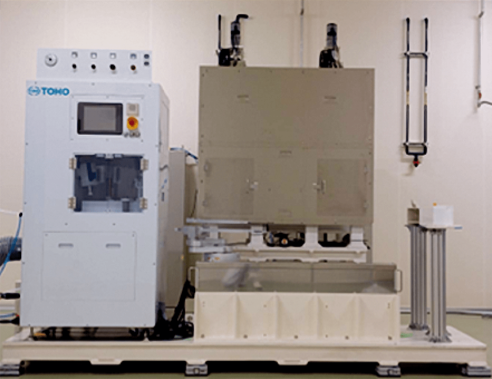
What does the system look like?
The single-platen single-head CARE-TEC® system (see figure below and the video showing the system in operation) is ready for customer demos at Toho for up to 150-mm substrates. The system comes with a post-cleaning module.
 .
.
The single-platen dual-head CARE-TEC® system (see figures below and the video showing the system in operation) is also ready for customer demos at Toho for 200-mm substrates. The system comes with a post-cleaning module.
![]() .
.
![]() .
.
![]() .
.
What is the main problem that CARE-TEC® is solving?
To best explain the need for CARE-TEC®, let’s take a look at the main unit operations for producing epi-ready SiC substrates (especially Steps 4, 5, 7, 8, and 9):
Steps 4, 5, and 7 add to the density of surface and subsurface defects, while Steps 8 and 9 result in far-from-ideal final surface finishes as both cause the formation of large numbers of lateral and vertical cracks within the plastic zone of the substrate and beyond (see the schematics and figures below):

What does our solution look like?
Araca’s approach to solving the above problem is two-fold:
First, with our patented hydrogen peroxide-based final buff slurry (PeroxSiC-100® – and available for sampling in July 2024), we are introducing a “CMP Final Buff Step followed by Cleaning and Inspection” after Step No. 9. This “gentle” slurry, with proprietary additives and abrasive nano-particles, and no potassium permanganate) buffs the surface to a nano-smooth mirror level (appx. 2 nm).
Next, we follow with the “CARE-TEC® Step” to further improve the nano-texture to below 1 nm with little to no surface and sub-surface damage. The final buff step can be skipped if the surface finish needs have been met with Step 9.
Results, using a Lasertec inspection system (see figure below), show the presence of 339 defects on a 150-mm “epi-ready” SiC substrate (left). After removing only 20 nm of SiC from the surface with CARE-TEC®, the total number of defects dropped to 95 (center). This slight thickness removal seems to have caused the appearance of subsurface latent scratches that could not be seen before our electrochemical CMP step. With the removal of another 80 nm of SiC using CARE-TEC®, the total number of defects dropped to only 31 (right) where most of the scratches and micro-cracks are no longer detectable.

.
Electrical results below show a dramatic improvement in gate leakage current (measured on multiple SBDs – Schottky Barrier Diodes) when CARE-TEC® is used. Applying CARE and CMP after activation annealing achieved approximately a single-digit or more reduction in leakage current density with a reverse voltage in the SBDs. The leakage current variation at – 600 V for the case of CARE-TEC® was the smallest of the three samples tested.

Gate Leakage Current: (left) without surface planarization, (center) with CMP and (right) with CARE-TEC®.
Source: Yamamoto et al. (2015)
Concerning time-dependent dielectric breakdown (TDDB) on MOS capacitors, again we see (figure below) significant benefits (orders of magnitude improvement) when CARE-TEC® is used. Applying CARE-TEC® and CMP, after deposition of a p-type epitaxial layer, achieved approximately single-digit or more improvement in the lifetime.

TDDB Data
Source: Yamamoto et al. (2015)
How to reach us?
For equipment pricing, to request additional information on CARE-TEC® and PeroxSiC-100®, and to schedule demos starting October 2024, please do not hesitate to contact us. We stand ready to serve you.